← Latest news 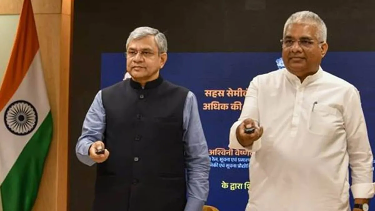
India inaugurates first SME-led semiconductor packaging facility in Rajasthan aiming to boost domestic chip output
Business
Published on 15 May 2026
Packaging starts with 60 million units a year
India inaugurated its first SME-led semiconductor chip packaging facility by Sahasra Semiconductors Pvt Ltd in Bhiwadi, Rajasthan, inside ELCINA’s Electronics Manufacturing Cluster at Salarpur, Khushkhera. Union Electronics and IT Minister Ashwini Vaishnaw said electronics production has surged to nearly Rs 13 lakh crore and exports to about Rs 4.24 lakh crore, with mobile phones now leading exports. The facility, backed under the SPECS scheme with investment over Rs 150 crore, uses Class 10K/100K cleanrooms.
- Facility inaugurated in Bhiwadi within ELCINA Electronics Manufacturing Cluster
- Virtual launch attended by Ashwini Vaishnaw, Bhajan Lal Sharma and Bhupender Yadav
- Built under the Ministry’s SPECS scheme with over Rs 150 crore investment
- Spans 57,000 square feet with Class 10K and 100K cleanrooms
- Annual packaging capacity starts at 60 million units, targets 400–600 million
- Over 60 percent output exported to markets including US and EU nations
Read the full story at Republic
This summarization was done by Beige for a story published on ![]() Republic
Republic